
-By Karan Shah
Capturing free-space optical light for high-speed Wi-Fi is an approach that captures the light from a large scale and funneling it into a narrow cone without losing speed. To view the visible path, it needs the plasmonic devices and a separate interior detector. This approach is achieved on small scale and now they try for a large scale with max high speed.
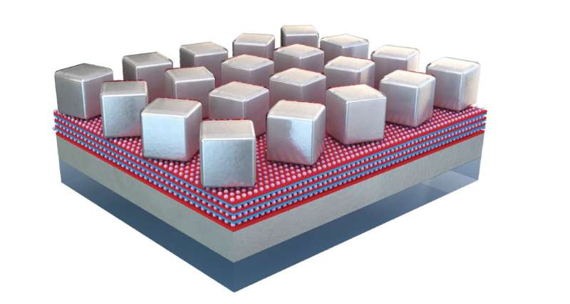
With help of the new type of fiber-optic wifi sensor, silver nanocube is placed above the silver base at a few nanometer distances and fluorescent dyes sandwiched in between. Nanocubes increase the photonic properties of the fluorescent dye.
Plasmonic increases the radiative properties of fluorescent materials by customizing the local density of states in practical optoelectronic applications due to losses and lack of scalability to macroscopic areas. Its speed enhancements to previously single nanostructure are duplicates on macroscopic devices increase up to 1,000-fold have been indicated for semiconductor quantum dots embedded in nanocube.
It is true that Infrared and visible light can indeed carry more data than radio waves but it’s limit up to wired, fiber-optic cable. Duke’s research team working with FaceBook’s connectivity lab has achieved to discard the fiber in fiber optics.
While working on optoelectronics to create a free-space optical communication system(FSOC) for wireless internet, the researchers also show that speed, lifetime, and efficiency properties of previously macroscopic areas demonstrated on the tiny, single-unit plasmonic antenna(sensor) can also be implemented on larger devices.
The research paper published on 11 Feb 2021 in the journal Optica and this mechanism was tested in a small chip.

Researchers created a new plasmonic metasurface, when light hits this structure; it excites surface plasmons, which causes the dye molecules to emit light very quickly after being excited by the incoming light and its structure in image b and wavelength in c and d Credit: Maiken H. Mikkelsen, Duke University.
Researchers from Internet.org’s FaceBook connectivity lab stated that a new type of light detector could be used for free-space-optical communication because it can be faster radio wave communications like wifi, Bluetooth. But the use of this kind of higher frequencies in wireless devices is more difficult, currently using the LED or laser as a detector can change the focus to optimize the connection and it would be much efficient.
Let’s take an experiment that was done in the lab, spherical packet of fluorescent fibers captured blue laser light in any direction and re-emitted green light that could be funneled onto a small optical receiver by achieving the speed of 2GB per second. Most fiber optic internet gives the speed up to 10 GB. For practical applications, a large effective area is used for an optical receiver for maintaining a fast response time. To achieve a large area scale, this is replaced by an achromatic lens with a focal length of 200 mm.
Increasing the speed of the model, the Connectivity Lab turned to Maiken Mikkelsen, the James N. and Elizabeth H. Barton Associate Professor at Duke University. Over the years, Mikkelsen’s research topic was plasmonics, which focuses the light into one tiny nanotube by transmitting and absorbing light to increase the device’s speed and efficiency up to 1000 times.
“The Connectivity Lab’s prototype was constrained by the emissions lifetime of the fluorescent dye used is very slow and inefficient,” said Mikkelsen. “They wanted to extend the efficiency and found my work showing ultrafast response times in fluorescent systems. The research leads to efficiency rates were possible on single, nanoscale or very small systems, so we didn’t know if it could go to a centimeter-scale large detector.”
Mikkelsen explains all this stuff has been proof for only a single antenna These systems usually involve metal nanocubes placed into tens to hundreds of nanometers apart and placed just a handful of nanometers above a metal film and has historically cherrypicked just one cube for measurement.
In the new paper, Mikkelsen and Andrew Traverso, a postdoctoral researcher working with her, brought a new more useful, and optimized design to a large-area plasmonic device. Silver nanocubes are 60 nm wide placed over 200 nm apart, and covers the 17% surface of the device and on a 7nm polymer layer with embedded fluorescent dye into the silver film that is overflowing the four layers of fluorescent dye.
The nanocubes interact with the silver base to increase the photonic properties of the fluorescent dye, this large-area metasurface composed of fluorescent dye coupled to nano patch antennas, exhibits a 910-fold increase in the overall fluorescence and a 133-fold emission rate enhancement and record the overall efficiency is 30%.
“Plasmonic effects have been known to lose a lot of efficiency over a large area in practical demonstrations,” said Traverso. “But we’ve shown that you can take attractive ultrafast emission features of a nanoscale device and recreate it on a macroscopic scale. And our method is very easily transferrable to fabrication facilities. We can create these large-scale plasmonic metasurfaces in under an hour with pipettes and Petri dishes, just simple liquid depositions on metal films.”
Next researchers would need to several plasmonic devices together to cover all the area 360-degree field of view and once again include a separate interior detector for large scale with the researchers to see a viable path forward.
“In this demonstration, our structure acts to efficiently relay the photons from a wide-angle into a narrow-angle without losing speed,” said Mikkelsen. “We didn’t integrate a regular fast photodetector as the Connectivity Lab did in their original paper yet. But we solved the major bottleneck in the design and the future applications are very exciting!”
A new approach to on-chip design including high-data-rate FSOC, effectively providing new material for ultrafast optoelectronic and sensing components.
Reference:
- Andrew J. Traverso, Jiani Huang, Thibault Peyronel, Guoce Yang, Tobias G. Tiecke, Maiken H. Mikkelsen. Low-loss, centimeter-scale plasmonic metasurface for ultrafast optoelectronics. DOI: 10.1364/OPTICA.400731
- Phys.org


2 Responses
Good knowledge for optical fiber !!
Thank you for your comment. Dont forget to share our work.